No edit summary |
|||
| (19 intermediate revisions by 2 users not shown) | |||
| Line 8: | Line 8: | ||
==Description== | ==Description== | ||
[[File:PCB finished (1).jpg|thumb]] | |||
[[File:Pcbdokupic8.png|thumb]] | |||
[[File:Ezgif-6-46dbab99ab2a.gif|thumb]] | |||
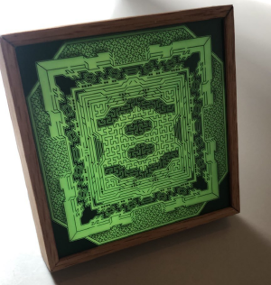
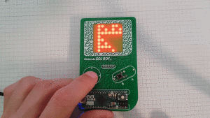
There is hardly an industrial process which is as optimized and streamlined yet customizable and complex as printed circuit board (PCB) production. At the same time it is highly accessible to anyone from electronic engineers to hobbyists, enthusiasts or artists thanks to very competitive and affordable prices and easy to use tools. Production files can be uploaded online for instant quotes. On submission customers can get real-time updates on the production process. | There is hardly an industrial process which is as optimized and streamlined yet customizable and complex as printed circuit board (PCB) production. At the same time it is highly accessible to anyone from electronic engineers to hobbyists, enthusiasts or artists thanks to very competitive and affordable prices and easy to use tools. Production files can be uploaded online for instant quotes. On submission customers can get real-time updates on the production process. | ||
| Line 16: | Line 19: | ||
Electrical functionality isn't a requirement for the result. The processes can also be utilized to create graphical works or the PCB can be a negative for relief printing processes. | Electrical functionality isn't a requirement for the result. The processes can also be utilized to create graphical works or the PCB can be a negative for relief printing processes. | ||
===German description=== | ===German description=== | ||
| Line 40: | Line 42: | ||
==Documentation== | ==Documentation== | ||
* [[/mxkllmnn/]] | |||
* [[/mxkllmnn (side project)/]] | |||
==Links== | ==Links== | ||
Previous classes from this series: | |||
* [[GMU:PCB Arts]] | |||
* [[GMU:Creative Circuit Boards]] | |||
===Software=== | ===Software=== | ||
* [https://kicad | * [https://kicad.org KiCAD] | ||
* [https://inkscape.org Inkscape] | * [https://inkscape.org Inkscape] | ||
* [https://github.com/badgeek/svg2shenzhen svg2shenzhen] | * [https://github.com/badgeek/svg2shenzhen svg2shenzhen] | ||
| Line 69: | Line 78: | ||
* [https://mitxela.com/projects/stylocard USB MIDI-stylophone business card] | * [https://mitxela.com/projects/stylocard USB MIDI-stylophone business card] | ||
* [https://tilde.industries tilde.industries] | * [https://tilde.industries tilde.industries] | ||
* [http://automato.farm/portfolio/believe_it_yourself/ automato.farm: Believe it Yourself] | |||
* [http://www.ww.crazywatches.pl/pulsar-calculator-time-computer-led-1975 Pulsar Calculator Watch insides] | * [http://www.ww.crazywatches.pl/pulsar-calculator-time-computer-led-1975 Pulsar Calculator Watch insides] | ||
* [https://wyolum.com/experimenting-pcb-rendering-using-kicad-freecad-and-blender PCB rendering workflow KiCAD-FreeCAD-Blender] | * [https://wyolum.com/experimenting-pcb-rendering-using-kicad-freecad-and-blender PCB rendering workflow KiCAD-FreeCAD-Blender] | ||
* [https://github.com/pcbarts/stylized-blender-setup pcbarts Blender setup] | * [https://github.com/pcbarts/stylized-blender-setup pcbarts Blender setup] | ||
* [https://kitspace.org kitspace.org] | |||
====Videos==== | ====Videos==== | ||
* [https://www.youtube.com/watch?v=NflYkVcWRRU PCB Art, A to Z] Alex Glow for Hackster.io | * [https://www.youtube.com/watch?v=NflYkVcWRRU PCB Art, A to Z] Alex Glow for Hackster.io | ||
| Line 79: | Line 91: | ||
====Tutorials==== | ====Tutorials==== | ||
* [https://svtronics.com/blog/what-is-the-difference-between-smt-smd-and-through-hole/ SMD | SMT | THT] PCB terminology | |||
* [https://prototypepcb.com/castellated-holes/ castellated holes] PCB terminology | |||
* [https://www.allpcb.com/mouse_bites_pcb.html mouse bites] PCB terminology | |||
* [https://www.protoexpress.com/blog/component-placement-guidelines-pcb-design-assembly/ PCB floorplanning] Improve your PCB design | |||
* [https://youtu.be/fYInlAmPnGo Soldering SMD] | |||
* [https://youtu.be/4GrQNH80oDY Soldering SMD] (funny german guy teaching electronics) | |||
===Components=== | ===Components=== | ||
Latest revision as of 11:03, 3 March 2022
Werk/Fachmodul
Lecturer: Max Neupert
Credits: 6 ECTS, 4 SWS
Date: Wednesday, 9:15 until 12:30h
Venue: Online
First meeting: Oct. 20
Moodle: 36608
Description
There is hardly an industrial process which is as optimized and streamlined yet customizable and complex as printed circuit board (PCB) production. At the same time it is highly accessible to anyone from electronic engineers to hobbyists, enthusiasts or artists thanks to very competitive and affordable prices and easy to use tools. Production files can be uploaded online for instant quotes. On submission customers can get real-time updates on the production process.
In the class Printed Circuit Board Art' we will explore printed circuit boards as a medium for artistic expression and will discuss and realize individual projects based on this investigation.
While doing so we will acquire an intermediate knowledge of the involved processes and learn how to use free software for schematic and PCB layout creation.
Electrical functionality isn't a requirement for the result. The processes can also be utilized to create graphical works or the PCB can be a negative for relief printing processes.
German description
Kaum ein industrieller Prozess ist so optimiert und perfektioniert, und dabei individualisierbar und komplex wie die Produktion von Leiterplatten. Gleichzeitig ist dieser Prozess für jeden zugänglich, ob Eletroniker*in oder Hobbyist*in, Enthusiast*in oder Künstler*in - dank einem starken Wettbewerb, erschwinglichen Preisen und einfach nutzbaren Werkzeugen. Die Dateien für die Produktion können hochgeladen werden um ein sofortiges Angebot zu erhalten. Nach dem Bezahlen kann der Kunde in Echtzeit den Produktionsverlauf nachverfolgen.
Im Kurs Printed Circuit Board Art werden Leiterplatten als ein Medium für künstlerischen Ausdruck erforscht und individuelle Projekte auf der Basis dieser Erkenntnisse realisiert.
Dabei werden wir fortgeschrittenes Basiswissen über die Prozesse erwerben und lernen wie freie Software zum Erstellen von Schaltplänen und Platinenlayout verwendet wird.
Elektrische funktionen sind keine Bedingungen für das Resultat. Der Herstellungsprozess für Leiterplatten kann auch dafür verwendet werden umd grafische Ergebnisse zu erzielen oder die Leiterplatte kann zu einem Stempel für Druckprozesse werden.
Topics
- Introduction to PCBs. Materials, layers, variants, production process
- Examples of PCBs including PCB art
- KiCAD making an schematic with eeschema
- KiCAD assigning footprints
- KiCAD laying out the PCB with pcbnew
- Inkscape introduction
- From Inkscape to KiCAD with svg2shenzhen
Evaluation
Active participation, presentation, artistic examination, documentation, edits in the wiki.
Documentation
Links
Previous classes from this series:
Software
- KiCAD
- Inkscape
- svg2shenzhen
- gerbolyze
- Stretch
- FreeCAD
- KiCADStepUp Workbench for FreeCAD
- PCBModE (Warning: Python 2.7 based!)
Circuit Simulation
- Circuitjs on Falstad.com Online simulator
- NGSpice / LTSpice / MacSpice
- YourSpice Spice models and circuits
- KiCAD spice model repository (unoffical)
Inspiration
- A History of Badgelife, Def Con’s Unlikely Obsession with Artistic Circuit Boards Daniel Oberhaus
- Badgelife: the art of the conference badge Jenny List
- #badgelife on Twitter
- Picoplanet, a generative PCB layout by bleeptrack
- Kelly Heaton
- Boldport Saar Drimer
- 8bitmixtape
- Andrew Sowa
- USB MIDI-stylophone business card
- tilde.industries
- automato.farm: Believe it Yourself
- Pulsar Calculator Watch insides
- PCB rendering workflow KiCAD-FreeCAD-Blender
- pcbarts Blender setup
- kitspace.org
Videos
- PCB Art, A to Z Alex Glow for Hackster.io
- Understanding & Making PCB Art Twinkle Twinkie DEF CON 27 talk
- Gonzo Circuits: The Synths of Peter B / Ciat-Lonbarde
- Getting to Blinky KiCAD tutorial
Tutorials
- SMD | SMT | THT PCB terminology
- castellated holes PCB terminology
- mouse bites PCB terminology
- PCB floorplanning Improve your PCB design
- Soldering SMD
- Soldering SMD (funny german guy teaching electronics)
Components
Manufacturing with online quote and processing
Comparison Sites and Directories
- PCB Market PCB comparison
- PCBshopper PCB comparison
- Directories: WLW, PCBdirectory
EU
- BETA Layout
- Aisler
- Multi-CB
- EMS
- Precoplat / MicroCirtec
- Fischer Leiterplatten GmbH
- EUROcircuits
- Soniclab
- PCB Joker using leftover space on production, but no control over parameters
- Omnitronik
Americas
- OSH Park
- American Standard Circuits (ASC) / Sunstone Circuits
- Sierra Circuits
- CircuitHub
- DigiKey Red


