No edit summary |
No edit summary |
||
| Line 10: | Line 10: | ||
I can hardly imagine a better „hello world of PCB design/art“. | I can hardly imagine a better „hello world of PCB design/art“. | ||
[[File:unicorn_render. | [[File:unicorn_render.png|800px]] | ||
'''Theme to be found:''' | '''Theme to be found:''' | ||
Revision as of 10:51, 3 March 2022
+ work in progress -
Introduction:
When I was browsing the university’s Bison portal for this semester’s offers, the PCB Art course caught my attention immediately, as I am passionate about electronics. To acquire the skill of making circuits on signature boards has been on my to-do list forever. Despite or precisely because I was actually supposed to be working on my final thesis this semester, the decision to take this course too was inevitable, especially since the software of choice in this course was KiCAD. The course title already gave it away, but at this point I did not know of the fascinating universe of PCB art and its huge community; not to mention the technical skills of making PCBs.
Hello World!
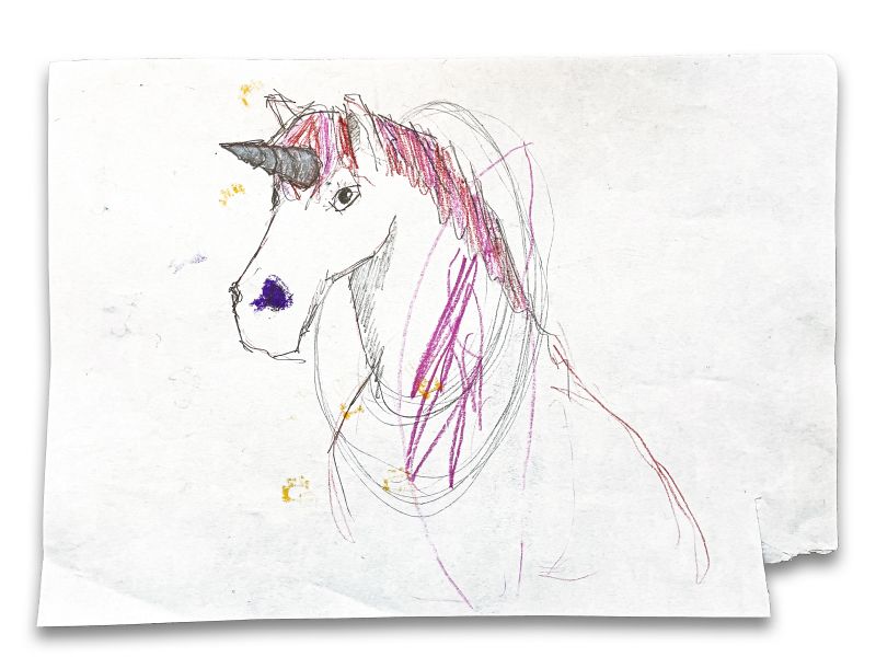
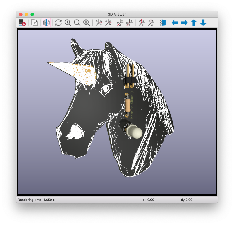
 Within tech culture, learning new skills usually starts with a so-called "hello world!" example. By accident there has been a sketch of a unicorn on my desktop when we started working on our very first PCB. So that unicorn happened to be the artwork template. It turned out to be a sophisticated application that was ideal for finding out how to create edge cuts, screen printing and mask layers in KiCAD. The initial circuit diagram was a luminous LED.
I can hardly imagine a better „hello world of PCB design/art“.
Theme to be found:
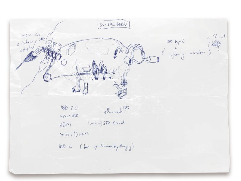
This design also led to my first project idea: Adaptors. That is because modern (read: Apple) computers (mine included) exist in a dream world where all its peripherals work with USB type C, whereas I find myself in the reality of 2022, where they do not. Everywhere I go I have to take many different adaptors to make my computer (that obviously supports USB type C only) work. So the idea was to have a unicorn (read: Swiss Army knife) to help out.  Unfortunately, when I teared down one of the adaptors available at the local electronics market, I found myself in a dream world. This time I realized that I do not have the electrical engineering degree I needed to understand the not-as-easy-as-I-thought circuitry of connecting different interface systems (HDMI/SD/Audio Jack/USB-A to USB-C). Even though it seems rather simple to transmit signals from one copper contact to another, many components are necessary in between. From the picture one can see that there is at least one IC per interface, as well as a quartz to translate between signals of different frequencies, not to speak of numerous capacitors, resistors and regulators.

The good thing about dismissing this first idea was the new opportunity to find a topic closer to what I was doing in my thesis at that moment. To call a spade a spade: I wrack my head around the question of how to cope with the challenge of increasing automation with regard to interfaces that are being transformed as a result. In most cases, if the cybernetic loop of control and display is being altered, a transformation of the underlying system’s user interface is implicit. In home automation, for example, this has led to the disappearance of well established interfaces and now all too often leave us frustrated. In a nutshell, this project is about designing new interfaces as an alternative to popular but dystopian smart home futures or: How to teach old switches new tricks.

