+ work in progress -
Introduction:
When I was browsing the university’s Bison portal for this semester’s offers, the PCB Art course caught my attention immediately, as I am passionate about electronics. To acquire the skill of making circuits on signature boards has been on my to-do list forever. Despite or precisely because I was actually supposed to be working on my final thesis this semester, the decision to take this course alongside was inevitable, especially since the software of choice was KiCAD. The course title already gave it away, but at this point I did not know of the fascinating universe of PCB art and its huge community; not to mention the technical skills of making PCBs.
Hello World!
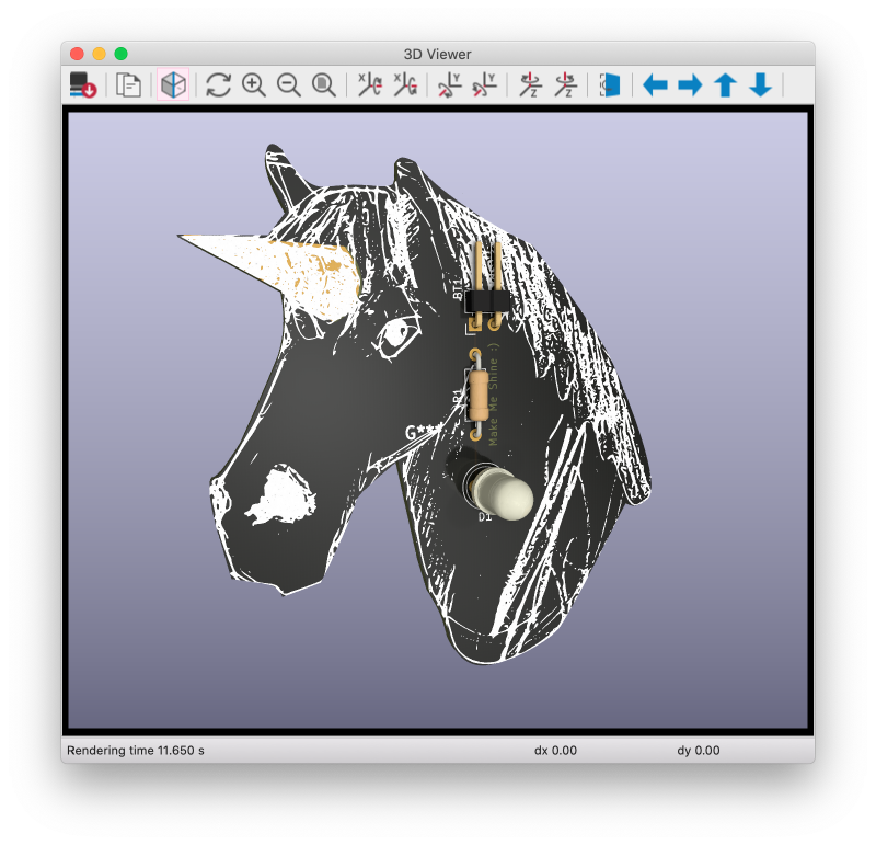
Within tech culture, learning new skills usually starts with a so-called "hello world!" example. By accident there has been a sketch of a unicorn on my desktop when we started working on our very first PCB. So that unicorn happened to be the artwork template.  It turned out to be a sophisticated application that was ideal for finding out how to create edge cuts, screen printing and mask layers in KiCAD. The initial circuit diagram was a luminous LED.
I can hardly imagine a better „hello world of PCB design/art“.
Theme to be found:
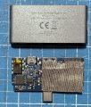
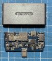
This design also led to my first project idea: Adaptors. That is because modern (read: Apple) computers (mine included) exist in a dream world where all its peripherals work with USB type C, whereas I find myself in the reality of 2022, where they do not. Everywhere I go I have to take many different adaptors to make my computer (that obviously supports USB type C only) work. So the idea was to have a unicorn (read: Swiss Army knife) to help out. 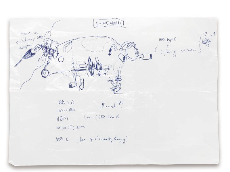 Unfortunately, when I tore down one of the adaptors available at the local electronics market, I found myself in a dream world. This time I realized that I do not have the electrical engineering degree I needed to understand the not-as-easy-as-I-thought circuitry of connecting different interface systems (HDMI/SD/Audio Jack/USB-A to USB-C). Even though it seems rather simple to transmit signals through copper traces, many components are necessary in between, if their ends do not speak the same language. From the picture one can see that there is at least one IC per interface, as well as quartz to translate between signals of different frequencies, not to speak of numerous capacitors, resistors, and regulators. So I started all over again.
The SwitchSwitch Concept:
When dismissing the first idea because it was not feasible for me in the time given, it seemed to be a good idea to work on something that already exists (or is in the making at least), namely the prototype I will be using as a platform for my thesis.
Very briefly, I wrack my head around systems whose user interfaces had to be modified as the result of process automation. In most cases, if the cybernetic loop of control and display is being altered, a transformation of the underlying system’s user interface is implicit. In home automation, for example, this has led to the disappearance of well-established interfaces and now all too often leaves us frustrated [1]. So I am exploring alternatives to popular but dystopian smart home futures, or: How to teach old switches new tricks.
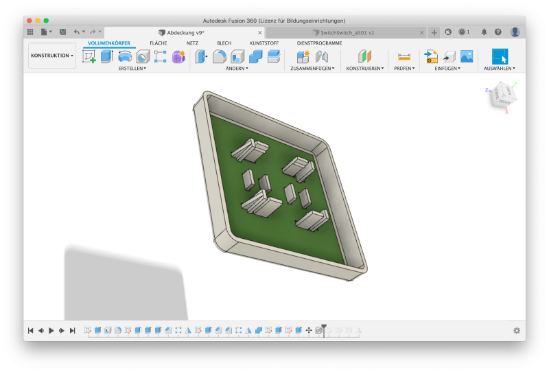
One idea for this course was to introduce capacitive touch areas – a formation of discrete sensor pads, sliders, or a matrix (see sketches below) – to the surface and the frame of a conventional switch, where the PCB itself serves as the cover. By that, one would extend the switch’s binary characteristic and broaden the repertoire of input gestures.
However, I soon realised that such a modification would undermine exactly what I am trying to preserve – the switching mechanism’s inherent psychophysical feedback that makes this kind of interface so appealing. Because the problem I am addressing is the replacement of great user interfaces (read: Switches, which are much more in line with our human sensory nature) by touch displays. This was an obvious choice, especially with regard to automation, as graphical user interfaces (GUIs) are much easier to integrate due to their ability to react to system changes simply by programming, whereas physical switches do not respond automatically. So the idea to have a remotely switchable switch was born, hence the working title SwitchSwitch. Furthermore, by temporarily decoupling the switch from the circuit of the object to be turned on or off and putting a microcontroller in between, the (automated) system becomes capable of utilizing the acoustic, visual and haptic signals evoked via the usage of its interface to articulate intent (at least this is the hypothesis to be confirmed). The SwitchSwitch prototype functions as a platform to design output gestures made of sequences of clicks in combination with flickering lights as means of communication. To do so a conventional switch has been equipped with some more advanced technology. Now this project is about turning this technology into an appropriate form.
Circuit & Components:
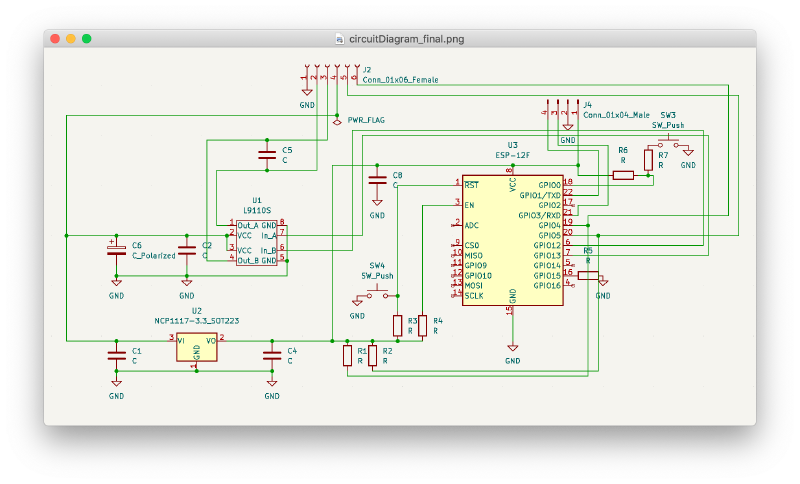
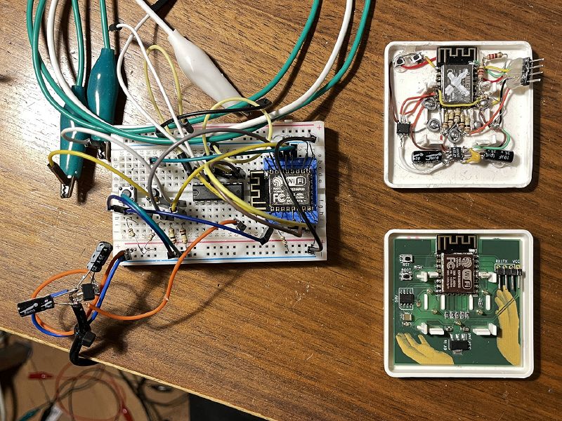
At this point, the switching mechanism has already been fully developed and all components were in place, although only on a breadboard. As the project is rooted in the smart home milieu, the decision on a microcontroller was easy: An ESP12 module based on the famous ESP8266 chip by espressif is the heart of the application. As mentioned before, GUIs can be altered by simply changing bits from zero to one or vice versa. Altering objects of the physical world requires kinetic energy. Therefore an electromechanical transducer is necessary. After many experiments, the decision was finally made in favour of a 12V DC brushed gearmotor. To control it with a microcontroller the L9110S H-bridge driver IC has been chosen. As the ESP runs on 3.3V a regulator IC (12V to 3.3V) was also to be installed as well as a couple of resistors, capacitors, and buttons.
Design:
The design was very much influenced by the early thoughts on the topic of "capacitive touch". I would have installed all the technical components in a dead bug fashion, disappearing into the flush socket of the wall, if it hadn't been for the idea of realising the entire backend as a PCB in the front, with touchpads on its rear. When the idea of touch input gestures was dropped (because this contrasted with highlighting mechanical devices), all that was left were components that logically belong to the backend. Yet, having everything fit tightly into the cover of the switch makes debugging very easy. By removing it, all the connections are accessible. So the transfer from breadboard to a PCB was the only logical consequence. To achieve this several steps have to be taken.
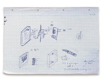
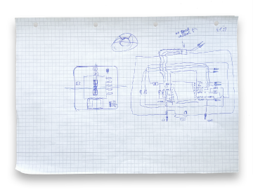
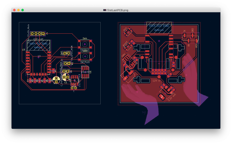
A milestone on this way is a hand-soldered prototype. As common switches come with a cover, the base plate already existed. But I did not start soldering right away. The first thing I did was a rough sketch of all components and their respective connections on a piece of paper. Only then I made my first attempts at this design in KiCAD. Since I did not want to spoil my option of revisiting capacitive touch gestures at a later stage, it was my personal challenge to realise everything on just one side of a PCB with no viases or through-hole components. Of course, this also meant that all elements had to be placed so that there is no intersection of a single trace, which has been hard before I got to know the practice of ground areas (across the entire PCB). Before the final layout was finished, it was an eternal back and forth between different media (KiCAD, paper, Fusion, soldering iron, and back again).
Still, this process was necessary to eliminate all the flaws of my design iteration by iteration, first and foremost an issue referred to as decoupling [2] [3]. This is of particular importance in my application as the ESP module is quite sensitive to noise and one of the worst components one can think of in terms of noise are motors. Here we have them combined on a tiny space of 50x50mm.
